 IC Device Repackaging
Overview
Original semiconductor devices are often constrained by legacy package formats that no longer align with updated system architectures, board layouts, or reliability requirements. As devices reach End-of-Life (EOL) or become unavailable in their original package configurations, repackaging becomes a critical engineering solution to restore compatibility, maintain functionality, and extend usable product lifecycles.
Outermost Technology delivers advanced, analysis-driven semiconductor repackaging services that enable existing packaged devices to be re-engineered into new configurations. Our expertise supports customers in overcoming End-of-Life (EOL) challenges, system requirement changes, and package conversion needs—while preserving device performance and reliability.
Backed by state-of-the-art facilities and deep engineering expertise, we provide a comprehensive repackaging solution encompassing precision decapsulation, die integrity evaluation, and customized re-packaging execution. Through advanced analytical and inspection capabilities—including microscopy, spectroscopy, X-ray inspection, and thermal analysis—we ensure technically sound decisions and controlled, repeatable outcomes. At Outermost Technology, repackaging is not just a process—it is a reliability-driven engineering discipline designed to extend product lifecycles and ensure long-term system stability.
Engage with Our Services for Optimal Solutions
Please see the table of service items below and contact us with your needs. You can also sign up to our portal site, which will make your job submission and work experience with us more efficient and convenient. If there are any services you don’t see on the table, please don’t hesitate to contact us. We are dedicated to identifying the most effective repackaging approach for your application and are always ready to extend our services to meet your specific requirements.
Process Flow
1. Incoming Inspection
Incoming Inspection is the first and most critical step in the semiconductor repackaging process. This stage establishes a technical baseline by evaluating the physical condition, package construction, and overall integrity of incoming devices prior to any invasive processing. Through systematic inspection and documentation, potential risks are identified early, enabling informed feasibility decisions and preventing downstream failure during decapsulation, analysis, or repackaging execution.
2. De-packaging
De-packaging is a critical step in the semiconductor repackaging process in which the original package materials are carefully removed to expose internal structures. This stage is performed using controlled mechanical and chemical techniques to access the die while preserving structural and functional integrity.
By applying package-specific de-packaging methods, potential damage to the die, bond pads, and interconnect structures is minimized. Proper execution at this stage is essential to enable accurate die inspection, analysis, and subsequent repackaging operations.
3. Die Cleaning & Inspection
Die Cleaning & Inspection is a critical step in the semiconductor repackaging process following de-packaging and die exposure. This stage focuses on removing residual contaminants and evaluating the condition of the die surface to ensure suitability for reliable reassembly.
Through controlled cleaning procedures and detailed inspection, surface contamination, material degradation, or physical damage can be identified before die attach and interconnection processes. This step establishes confidence that the die meets technical and reliability requirements for downstream repackaging.
4. Die Attach
Die Attach is a foundational step in the semiconductor repackaging process where the exposed die is securely bonded to a new substrate or lead frame. This stage ensures mechanical stability, proper thermal path, and electrical connectivity readiness before interconnection.
Precise control of materials, placement, and process parameters is essential to minimize void formation and ensure long-term reliability of the repackaged device.
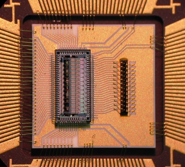
5. Interconnection
Interconnection is the stage in the semiconductor repackaging process where the die is electrically connected to the new substrate or package leads. This step ensures functional continuity between the die and the rest of the device, providing reliable electrical signal paths and enabling full device performance.
Accurate interconnect formation and verification are essential to minimize electrical failures such as opens, shorts, or signal degradation, and to support long-term reliability.
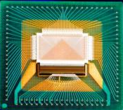
6. Molding & Encapsulation
Molding & Encapsulation is the process of protecting the die and interconnection structures by applying encapsulation materials designed to withstand mechanical, thermal, and environmental stress. This stage provides physical protection while maintaining package integrity and long-term device reliability.
Proper material selection and process control are essential to prevent defects such as voids, delamination, or material degradation that may impact device performance over time.
7. Marking
Marking is the process of applying permanent identification to the repackaged device for traceability, identification, and documentation control. This stage ensures that part numbers, lot information, and tracking data remain readable throughout handling and field use.
Proper marking execution prevents misidentification while minimizing surface damage or material interaction.
8. Electrical Testing
Electrical Testing verifies functional and parametric performance of the repackaged device. This stage confirms that repackaging has not introduced electrical defects and that the device operates within defined specifications.
Electrical testing provides confidence prior to shipment, qualification, or system integration.
9. Reliability & Inspection
Reliability & Inspection is the final verification stage focused on confirming long-term device stability and overall repackaging quality. This step integrates inspection, analytical review, and engineering judgment to support confident device reuse and lifecycle decisions.
FAQ
A: De-packaging is the precise process of removing original encapsulation or housing materials to expose the silicon die and its internal structures. This allows for detailed inspection, failure analysis, and subsequent repackaging into new formats.
A: Direct access to the die, bond pads, and interconnects is essential. De-packaging enables our engineers to evaluate the physical condition of the die and determine its suitability for the re-engineering process.
A: Die cleaning is essential for removing residual molding compounds, chemical byproducts, and microscopic contaminants. This ensures a clean surface that facilitates reliable die attachment and robust electrical interconnections.
A: Beyond structural support, die attach determines the thermal dissipation profile of the device. High-quality bonding ensures that heat generated during operation is efficiently transferred away from the die, preventing thermal degradation and ensuring long-term system stability.
A: Depending on the device architecture and performance requirements, we utilize:
- Flip-Chip Assembly: Utilizing solder bumps or copper pillars
- Wire Bonding: The most versatile method, using ultra-fine wires to connect bond pads to leadframes or substrates.
A: Yes. We utilize Non-Destructive Evaluation (NDE) tools such as Real-time 2D X-ray and 3D X-ray Computed Tomography (CT) to detect sub-surface anomalies like wire sweeping, cratering, or solder bridging.
A: We select encapsulants based on the target application’s mission profile:
- Epoxy Molding Compounds (EMC): The industry standard for high-volume, robust protection.
- Liquid Encapsulants / Glob-Top: Ideal for Chip-on-Board (COB) and specialized small-batch repackaging.
- High-Thermal Conductivity Compounds: Formulated with
A: Content is defined by customer requirements but generally includes:
- Part Number: Product identification.
- Lot Code: Unique batch identifier.
- Date Code: Manufacturing work week (e.g., 2604 for Year 2026, Week 4).
- Country of Origin: Legal manufacturing location.
- 2D Matrix/QR Code: For high-density automated data retrieval.
A: Not necessarily. The test coverage is defined by the Test Plan (TP). Some clients require full characterization, while others opt for a DC Parametric Test (checking for opens, shorts, and leakage) or a specific functional subset to verify the device survived the repackaging flow.
A: Yes, it provides Confidence Extension. By verifying that a repackaged or legacy component is structurally identical to a “new” part, we provide the technical justification needed to extend the service life of systems relying on discontinued or reconditioned semiconductors.