 Transmission Electron Microscopy (TEM)
Overview
Transmission Electron Microscopy (TEM) is a versatile tool that generates nano-scale imaging down to atomic level along with compositional information. With TEM, an electron beam is transmitted through a sample and then magnified and focused onto a fluorescent screen forming high-resolution images. To prepare a sample thin enough, between 50 nm ~ 100 nm thick, the use of Focused Ion Beam (FIB) equipment is required, which is a critical step that significantly affects the data quality and images.
- Imaging
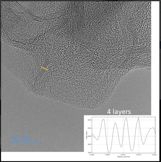
- HR-TEM: High Resolution (HR)-TEM which allows imaging down to 10-9 m scale.
- Cs-TEM: Spherical Aberration Corrected (Cs)-TEM which generates super high-resolution images down to 10-10 m scale.
- STEM: Scanning Transmission Electron Microscope (STEM), which is a different mode of imaging available with both HR- and Cs- TEM. While TEM uses a parallel electron beam passing through a specimen, STEM uses a convergent beam which makes STEM suitable for composition analytical techniques such as energy dispersive X-ray (EDS or EDX) spectroscopy or electron energy loss spectroscopy (EELS).
- Composition
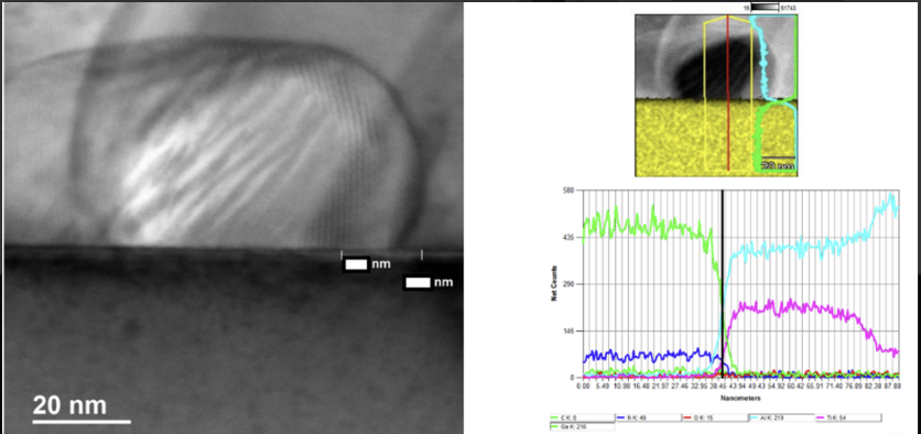
- EDS: EDS provides compositional information through the analysis of X-rays generated by the electron beam. EDS spectrum includes the information for all the elements within the scanned area.
- EELS: EELS uses energy loss of the inelastically scattered electrons and provides good sensitivity for the lighter elements.
- Structure
- Imaging: TEM provides images in various magnification, from atomic to micrometer scale, which shows sample specific structure information for both organic and inorganic materials.
- Transmission Electron Diffraction (TED): From the nature of TEM using focused electron beam, TED can provide information about crystal lattice constants, defects, or unknown structure developed during some process.
To read more on TEM, you can read our Key Tech brochure.
Services
TEM is widely used for exploration of nanostructure and composition analysis in various industries such as semiconductor, LED, graphene, photovoltaic, and bio industries.
- Imaging in wide range of scales focused on the structure information down to atomic scale.
- Composition: EDS and EELS analysis generates elemental information for raw materials and electronic devices.
- Crystallographic analysis using TED and EBSD analysis
Equipment
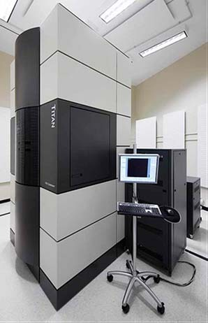
The FEI Titan Themis 3 is a high-resolution transmission electron microscope, which can operate in both TEM and STEM modes.
- Extreme Field Emission Gun with Brightness 7×10⁷A/m2 sr V, Current (≥ 50nA before Monochromator), Current Stability, Spatial Coherency, and Temporal Coherency
- Monochromator with Energy resolution at 300KV ≤ 0.2eV
- Accelerator at 60 to 300 kV
- 3 Lens Condenser
- DCOR Probe Cs Corrector
- Super-Twin Objective Lens
- Super-X Detector (4 Silicon Drift Detectors)
- CETCOR Image Cs Corrector
FAQ
A: The difference between TEM cross-section and plan view is the lamella preparation. For cross section the lamella is cut down the z-direction (vertical) thus the TEM Image will be the cross section of the sample, usually visualizing multiple layers. As with plan view the cross section is made through the x-y (horizontal) direction thus the TEM image is of plane rather than a cross section. Deciding between the two lamella preparations comes from the location and features you are interested in analyzing.
A: TEM is a microscopy technique that uses a beam of electrons to transmit through an ultra-thin sample, creating high-resolution images. It operates on the principle of electron wave interference.
A: STEM is a variation of TEM where a focused electron beam is scanned across a specimen to form an image. In contrast, TEM forms images by transmitting electrons through the entire sample. STEM provides compositional information and can be used for high-resolution imaging.
A: EDS is an analytical technique used in TEM to determine the elemental composition of a sample. It detects X-rays emitted when the electrons from the electron beam interact with the sample, providing information about the elements present.
A: EELS is an analytical technique used to analyze the energy loss of electrons passing through a sample. It provides detailed information about the chemical bonding and electronic structure of the material.
A: EDS provides information about the elemental composition of a sample, while EELS offers insights into the chemical bonding and electronic structure. EDS is often used for qualitative elemental analysis, while EELS provides quantitative data.
A: Cross-sectional analysis involves preparing a thin section of a material perpendicular to its surface. TEM is used to examine the internal structure and layers of materials, including semiconductor devices, integrated circuits, and biological samples.
A: Plan view analysis involves examining a material’s surface or a thin section parallel to the surface. It is used to study surface structures, interfaces, crystallography, and defects in materials.
A: TEM offers nanoscale resolution, allowing researchers to visualize and analyze materials at the atomic and molecular levels. It is essential for characterizing nanoparticles, nanomaterials, and nanostructures.
A: Sample preparation for TEM involves thinning the sample to electron transparency. This often includes techniques such as ultramicrotomy, ion milling, or focused ion beam (FIB) milling.
A: TEM requires samples to be extremely thin, limiting its application to bulk materials. It also operates in a high vacuum, which may affect the analysis of certain materials. Additionally, electron radiation damage can be a concern, especially for sensitive samples.