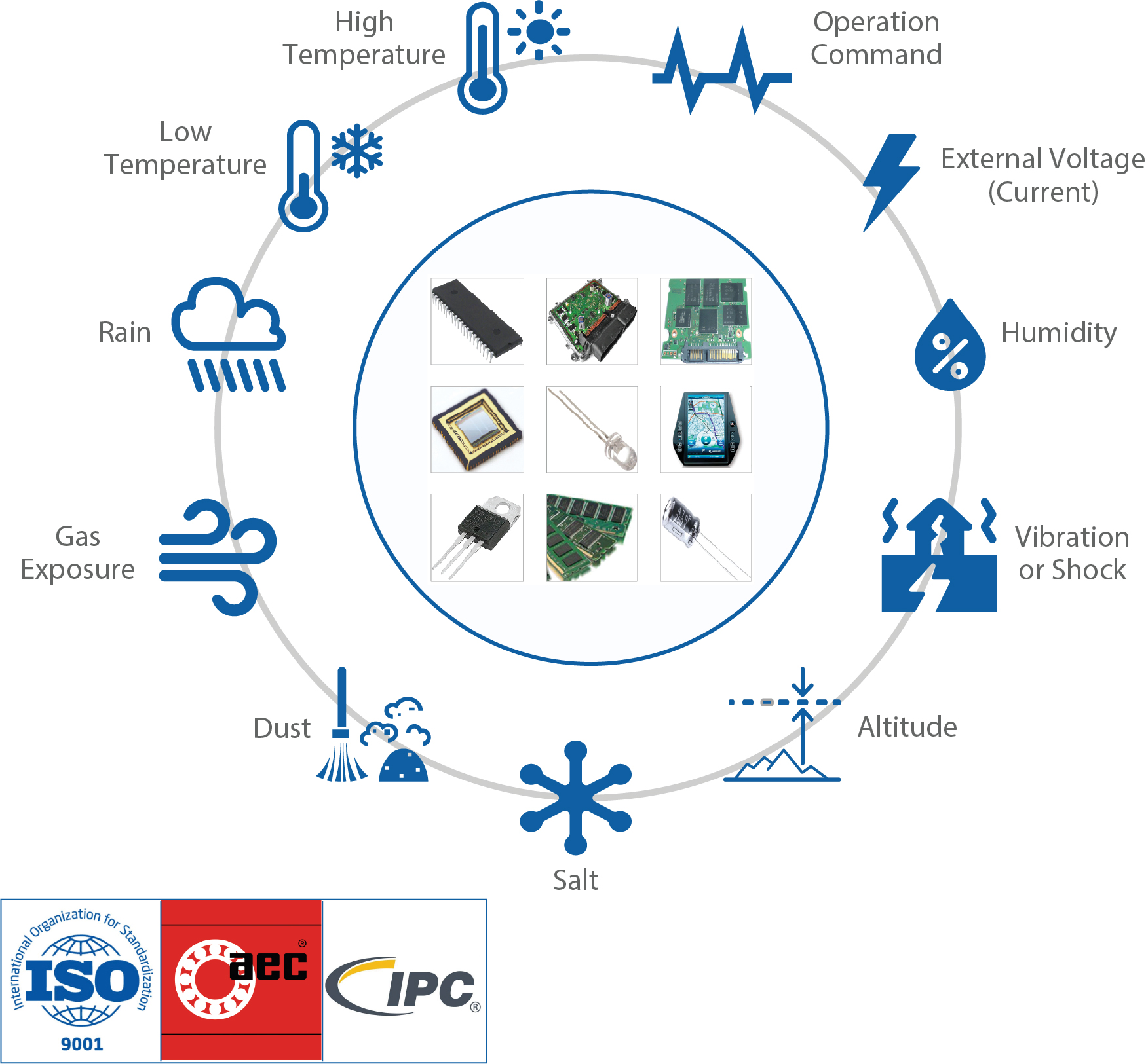
Reliability Testing
Reliability is defined as the ability of a device to conform to its electrical and visual/mechanical specifications over a specified period of time under specified conditions at a specified confidence level. Reliability engineering employs a wide variety of reliability tests like the lifetime, environmental including humidity, electrical, thermal, mechanical testing. RT is often divided into the wafer level RT and package level RT, too. Wafer-level RT is when the first silicon comes out to check the reliability issue at the early stage. Package level RT uses one or more of the following stress factors to accelerate failure: temperature, moisture or humidity, current, voltage, and pressure. The most popular industry-standard reliability tests for semiconductors are already available. Outermost Technology provides the testing services for your chips’ reliability and provides the engineering consulting for failure analysis and design for reliability.
| Tested Environmental Conditions | |||
|---|---|---|---|
 | |||
| Mechanical Shock | 340 g – 10,000 g; 5 shocks per orientation; JESD22-B110B |
| Vibration & Resonance | 20 Hz – 2000 Hz, 4 cycles for 3 axis; 12 cycles total; JESD22-B103B |
| Universal Testing Machine | Shear, pull, edge break, body strength, 3 points bending tests |
| Bending | Speed: 20 mm/min; JESD22-B113 |
| Torsion & Free Drop | 1 Hz/25 times & 1.0 mm/min speed |
| HALT | Optional temperature & vibrational stressing, IPC9592A |
| Early Life Failure Rate | T ≥ 125°C; 48 hrs ≤ t ≤ 168 hrs; ELFR-JEDEC/ELFR-AEC-Q100-008 |
| HTOL | 125°C; 1008 hrs; other conditions available; JESD22-A108 |
| LTOL | -65°C; 1008 hrs; other conditions available; JESD22-A108 |
| Erase and Write | 125°C;168 hrs; other conditions available; JESD22-A117/AEC-A100-005 |
| PLT | 25°C; 1008 hrs; other conditions available; JESD22-A108 |
| Temperature Cycling | -65°C to +150°C; other conditions available; TC-JEDEC/TS-Mil-Std-883 |
| Thermal Shock | -65°C to 150°C; JESD22-A106/Mil-Std-883, method 1011 |
| THB | 85°C, 85% RH, 1000 hrs; other conditions available; JESD22-A101 |
| HTS | +85°C to +300°C; JESD22-A103/Mil Std 883, method 1008 |
| LTS | -65°C to -40°C; JESD22-A119/EIAJ ED-4701/200, test method 202 |
| HAST | 130°C, 85% RH, 96 hrs; other conditions available; JESD22-A110 |
| Pressure Cooker Test | 121°C, 100% RH, 96 hrs; other condittions available; JESD22-A102 |
| Salt Atmosphere Test | [Salt]: 0.5% to 3%; JESD22-A107/Mil-Std883, method 2005 |
| Preconditioning of SMD | Prior to THB, HAST, TC, AC, and UHST; JESD22-A113/JSTD-020 |
| Moisture Sensitivity Level | Level 1 to 6; JSTD-020 |
| Design for Excellence (DFX) | Advanced design for analysis, debug, manufacturing, reliability, test, service |
| Failure in Time (FIT) | Failure rate that occurs during one billion device hours |
| Failure Mode and Effects Analysis (FMEA) | Evaluate failure occurrence, detectability, severity and consequences |
| Acceleration Factor, Temperature (AT) | Calculated from activation energy, Boltzmann constant, stress T, failure rates |
| Mean Time Between Failure (MTBF) | Predicted from bill of materials (BOM), stress analysis and AT |
| TeraBytes Written (TBW) | Estimate the total amount of data that can be written to the NAND device in its lifetime |